MEMS Foundry Service
概述
索尼半导体解决方案株式会社利用长年积蓄的MEMS/半导体加工技术与MEMS代工实绩,广范围地提供从试制到量产的“一条龙”MEMS代工服务。支援客户的MEMS开发及生产需求。
・Foundry services
Wafer process development (development, engineering samples, low ~ high volume mass production)
・Available processes
Bulk process (including SOI), surface process, semiconductor process.
・Fab Location
Sony Semiconductor Manufacturing Corporation, Kagoshima Technology Center
・ISO Certifications
ISO9001、ISO14001
MEMS Foundry Customer Engagement Flow
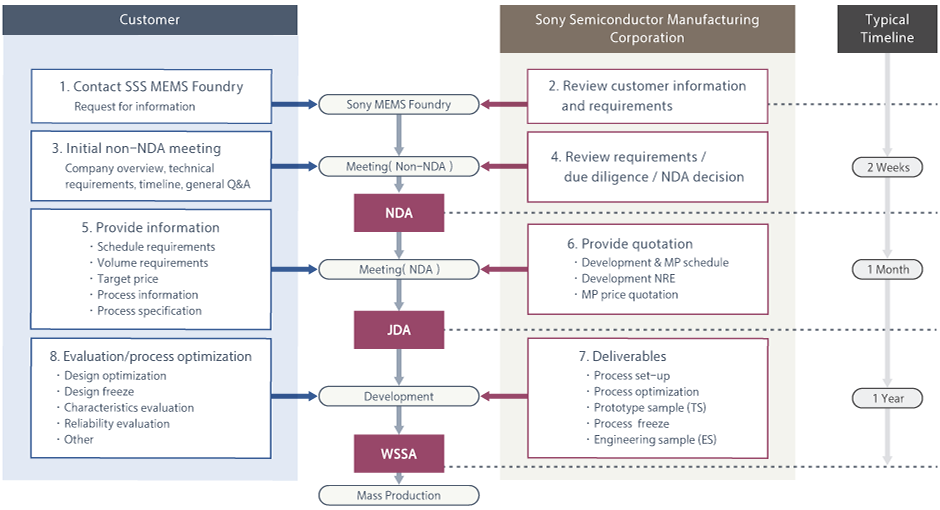
*) 本时间表仅作参考,可能会因产品及开发项目而不同,敬请谅解。
JDA: Joint Development Agreement
WSSA: Wafer Supply & Services Agreement
特点
服务与设备
| MEMS Foundry service (as of Apr.2022) | |
|---|---|
| Location | Kirishima City, Kagoshima Prefecture, Japan |
| Clean class | Class 1-1000 |
| Wafer size | 8inch |
| Production capacity | Small volume engineering samples - mass production |
| Services | Process optimization, Engineering samples, Mass production |
| ISO, etc. | ISO9001, ISO14001 |
| Development / Production experience | various sensors, actuators, optics |
| Process technology | Bulk processing including SOI, Cavity-SOI, Surface processing |
| Equipment | |
|---|---|
| Photolythography | Stepper, Double sided aligner, Coater, Developer |
| Heat treatment / diffusion | Diffusion, Ionic diffusion |
| Deposition | LPCVD, PCVD, Sputter, Vapor deposition, Doped Poly, Epi Poly |
| Dry etch | RIE, DeepRIE, Asher |
| Wet etch | HF, KOH, Resist removal |
| Cleaning | RCA, Organic cleaning |
| Other | Plating, Lift off |
| LowStress SiN, LowStress Poly, LowStress Epi Si | |
| Epi | |
| Design / Analysis | Analysis environment |
| Measurement / Evaluation | MEMS measurement, Evaluation environment |
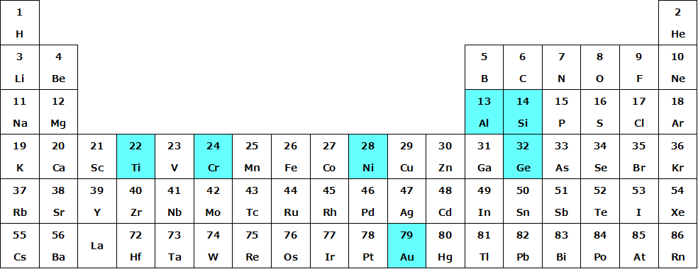
支持广范围材料
Process technologies
也支持其他各种设备结构,敬请咨询。
◆TSV (Through Silicon Via)
这是1项实装技术,是垂直贯通硅芯片内部的电极。当多枚芯片堆叠成1个封装,可期待能通过此贯通电极连接上下各芯片,实现封装的小型化并提高可靠性。
Features
・High aspect ratio TSV
・High-density TSV
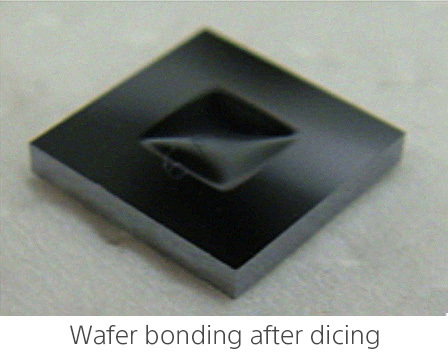
◆WLP (Wafer Level Package)
通过晶圆键合技术,可实现包括封装在内的MEMS芯片的小型化。
Features
・Au - Si Eutectic Bonding
・Vacuum Sealing
・Au - Au Bonding
・Glass Frit Bonding
・Resin Bonding
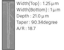
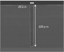
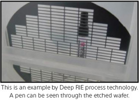
◆Deep RIE Process
(Deep RIE)是反应性离子蚀刻 (RIE) 的一种,是指高纵横比(窄、深)反应性离子蚀刻。由于其纵横比高,也被称为高纵横比蚀刻。
是MEMS体微加工的主要制作技术。
Features
・High aspect ratios
・Various taper angles
・Filling
◆Epi Poly Process
可以在构造体上形成Epi Poly层,进而形成构造体。能实现复杂的设备结构。
Features
・Thick Poly-Si
・Low-resistance Poly-Si
・Low-stress Poly-Si
联系我们
有关索尼半导体解决方案集团以及产品、服务的咨询和规格、报价/采购等请求,请点击下方按钮填写专用表格与我们联系。